


Choosing the Right Probe for Power-Electronics Applications
Source: Probemart 2026-04-30 Views: 183
Power conversion technology
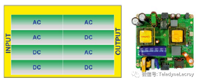
Power converters convert the attribute values of input energy (such as amplitude, frequency, and phase) into other values desired at the output. In modern industry, performance requirements for various power converters are becoming increasingly stringent in terms of capacity, voltage class, efficiency, and size (issues related to switching frequency).
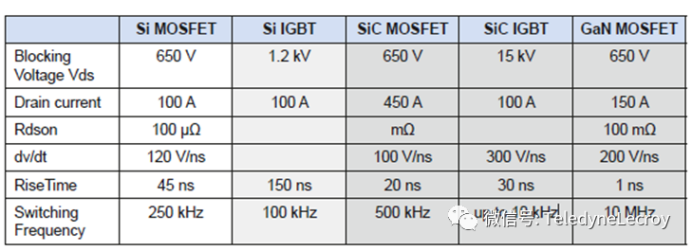
To improve the performance of existing power converters, use wide-bandgap (WBG) switching devices to replace conventional silicon switching devices; gallium nitride (GaN) high-electron-mobility transistors (HEMTs) and silicon carbide (SIC) metal-oxide-semiconductor field-effect transistors (MOSFET) are currently the most commonly used wide-bandgap (WBG) semiconductor materials. Wide-bandgap semiconductor materials have superior properties to silicon materials.
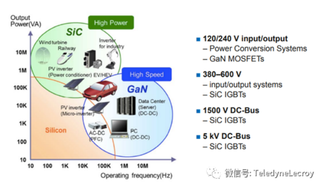
The advantages of wide-bandgap semiconductors enableGaN HEMToperation at low power () to medium power () applications have been more widely adopted,SiC MOSFETis more suitable for medium-power () to high-power (>10 kW) applications.
Currently,GaN HEMTits advantages have not yet been fully utilized, becauseGaNand the substrate have a relatively large thermal resistance, which leads to self-heating issues and may cause the switching device to overheat. However,GaN HEMTcan provide higher efficiency and switching speed,SiC MOSFETprovides higher voltage, current, and temperature characteristics.
The main challenge in using wide-bandgap semiconductor switching devices is to overcome the potential problems caused by their high slew rates, which may degrade electromagnetic interference (EMI) levels and may cause voltage oscillations and instability.
It can be stated with certainty that the standard passive probe supplied with the oscilloscope is not suitable for general power analysis. Such applications require a more specific solution, which is defined by the probing technique you intend to use and the type of power device to be tested.
The following are power device types commonly used in power-electronics applications. Understanding which types of power devices are used in your product is the first step in selecting the correct probing solution. LeCroy offers the industry's most comprehensive probe portfolio, so you can select the appropriate probe for your application for testing.
How do you select the correct probe for a specific measurement requirement?
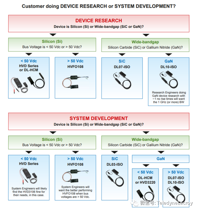
A simple way to determine the best probe for power-conversion probing is: first, determine whether you are conducting power device research or system development.
Second, determine the type of power device used (silicon or wide-bandgap semiconductor). If it is silicon, determine the voltage; if it is a wide-bandgap semiconductor, determine whether the device used isSiCorGaN。
Vds and Vgs measurement

Probe selection depends on:
■ Measurement of the high-side or low-side switch in a half bridge
■ Voltage range
–Automotive:48 V
–Power supply:>100 V
■ Switching frequency/Rise time
–SiCorGaN
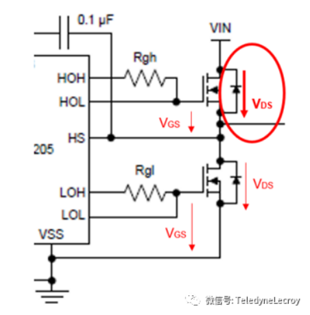
High-side switch of the half-bridge
–voltage not referenced to ground
Low-side switch of the half-bridge
–voltage with respect to ground
load
–high voltage
Probe applications
When performing different power-analysis applications, probes can provide different measurement accuracy. The following are the recommended LeCroy probes for different applications.
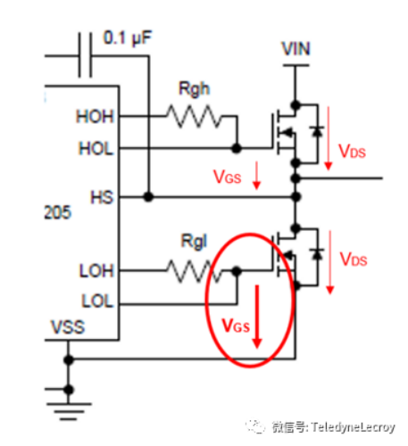
01 Low-side switch measurementVgssignal
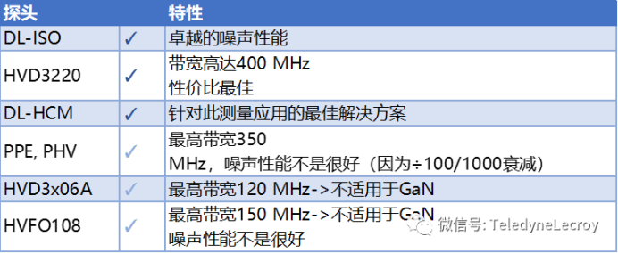
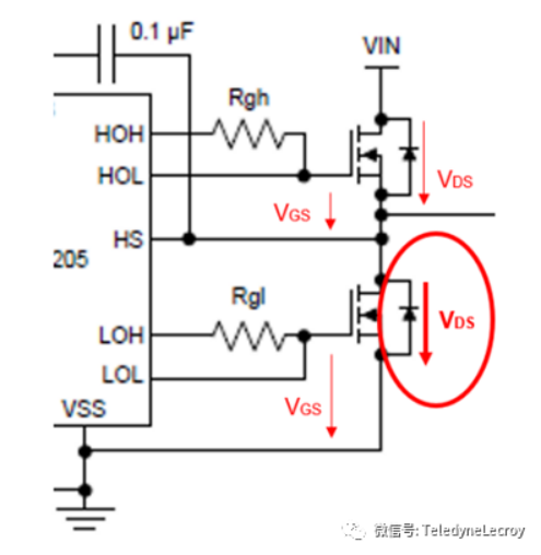
02 Low-side VDS signal measurement

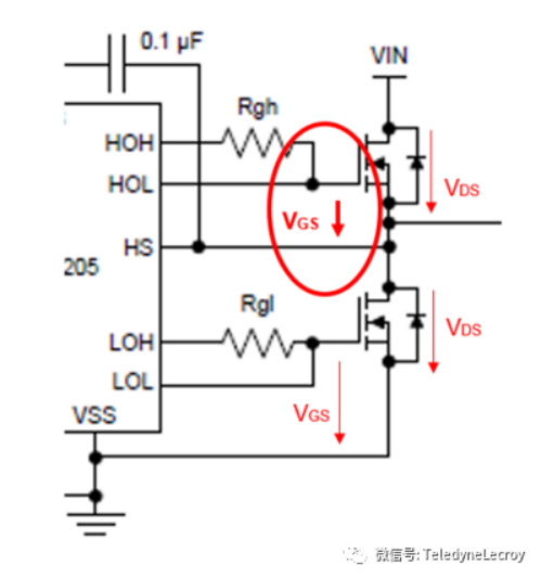
03 High-side switch measurementVgssignal
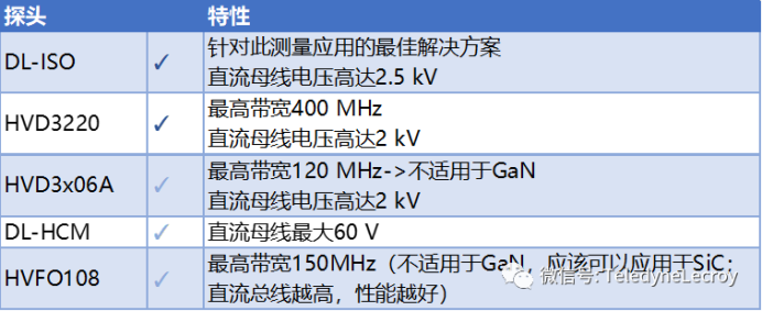
04 High-side VDS signal measurement

Measurement setup
The setup shown in the figure includesWavePro 804HDoscilloscope,T3AWG3352arbitrary waveform generator,DL10-ISOoptically isolated probe,DL10-HCMhigh common-mode probe,CP30Acurrent probe andInfineon GaNhalf-bridge evaluation board. The board is powered by a single 5 V supply from the T3PS3000 power supply (not shown).


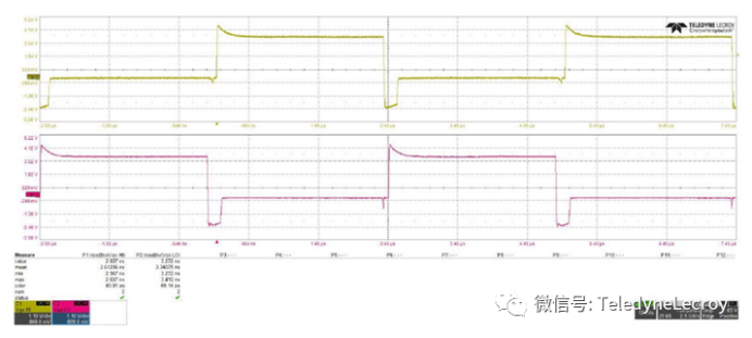
T3AWG3352 provides a PWM input, and the board can operate up to 2 MHz. The DL10-ISO probe is used to measure the high-side gate, while the DL10-HCM probe is used to measure the low-side gate. The bus voltage is also provided by the T3PS3000, but the voltage is limited to 40 V; the output current waveform is measured with the CP30A current probe.
The figure below shows the high-side gate captured with DL10-ISO and the low-side gate captured with DL10-HCM.

PCIM Europe 2026, Nuremberg: IWATSU and PMK at Booth H7-157
2026-06-15
APEC 2026: 41st IEEE Applied Power Electronics Conference and Exposition
2026-03-15
Semicon China 2026, Shanghai New International Expo Centre (SNIEC)
2026-03-11
WiPDA Asia 2025, Beijing International Convention Center, 15 August
2025-08-06